| CPC H03H 11/04 (2013.01) | 8 Claims |
|
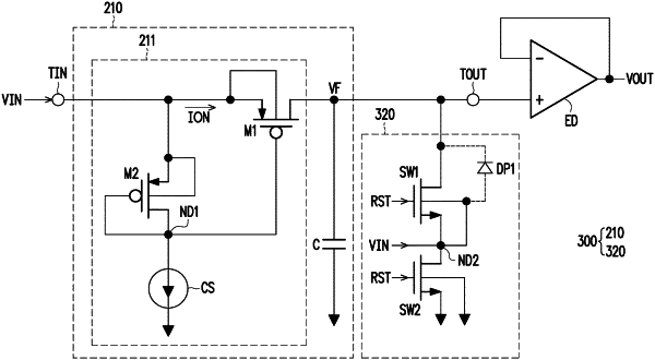
1. A low-pass filter circuit, comprising:
a low-pass filter, coupled between an input terminal of the low-pass filter circuit and an output terminal of the low-pass filter circuit, configured to receive an input voltage signal through the input terminal during a first period, performing a low-pass filter operation on the input voltage signal to generate a filtered voltage signal, and providing the filtered voltage signal to the output terminal; and
a discharging circuit, coupled between the output terminal and a reference low voltage, configured to receive the input voltage signal during the first period, and suppressing a leakage current flowing between the output terminal and the reference low voltage according to the input voltage signal and a reset signal,
wherein the discharging circuit comprises:
a first discharging switch, wherein a first terminal of the first discharging switch is coupled to the output terminal, a second terminal of the first discharging switch is coupled to a connection node, and a control terminal of the first discharging switch is configured to receive the reset signal; and
a second discharging switch, wherein a first terminal of the second discharging switch is coupled to the second terminal of the first discharging switch, a second terminal of the second discharging switch is coupled to the reference low voltage, and a control terminal of the second discharging switch is configured to receive the reset signal,
wherein during the first period:
supply of the reset signal is stopped, such that both the first discharging switch and the second discharging switch are turned off, and
the input voltage signal is provided to the connection node, such that a voltage value of the connection node is pulled up in response to the input voltage signal.
|