| CPC H01L 33/62 (2013.01) [H01L 27/156 (2013.01); H01L 33/005 (2013.01); H01L 33/50 (2013.01); H01L 33/60 (2013.01); H01L 2933/0058 (2013.01); H01L 2933/0066 (2013.01)] | 10 Claims |
|
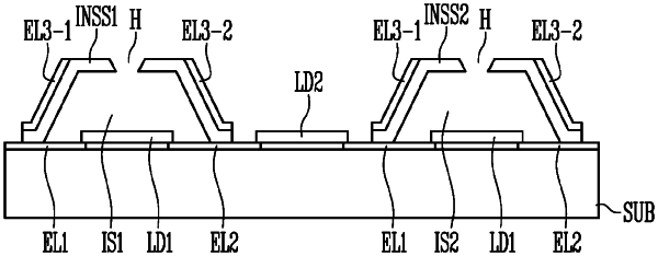
1. A method of manufacturing a display device, the method comprising:
forming a first electrode and a second electrode on a substrate;
forming at least one pattern on the substrate to have a convex shape with respect to the substrate and to expose a portion of the first electrode and a portion of the second electrode;
sequentially forming an insulating layer and a conductive material layer on the substrate;
patterning the conductive material layer to form a third electrode exposing a portion of the insulating layer;
patterning the insulating layer to form a hole exposing the at least one pattern;
removing the at least one pattern from the substrate to form at least one insulating structure having the convex shape with respect to the substrate;
providing a first light emitting element for emitting light in the at least one insulating structure; and
aligning the first light emitting element between the first electrode and the second electrode.
|