| CPC H01L 33/38 (2013.01) [H01L 33/382 (2013.01); H01L 33/387 (2013.01); H01L 33/405 (2013.01)] | 15 Claims |
|
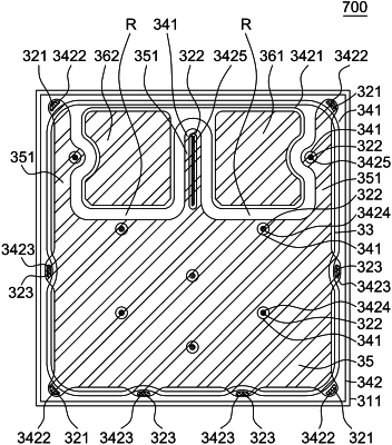
1. An optoelectronic device, comprising:
a semiconductor stack comprising a first semiconductor layer, a second semiconductor layer, and an active layer formed between the first semiconductor layer and the second semiconductor layer, wherein in a top view of the optoelectronic device, the first semiconductor layer comprises multiple boundaries, a peripheral frame region and multiple internal regions, wherein the peripheral frame region and the multiple internal regions are not covered by the active layer and the second semiconductor layer, and wherein the peripheral frame region is adjacent to the multiple boundaries and encircles the second semiconductor layer, and the multiple internal regions are surrounded by the second semiconductor layer;
a first insulating layer formed on the semiconductor stack and comprising a plurality of first openings exposing the first semiconductor layer, wherein the plurality of first openings comprise a first group on the multiple internal regions and a second group on the peripheral frame region;
a third electrode formed on the first insulating layer and comprising a first extended portion and a plurality of second extended portions connected to the first extended portion, wherein the first extended portion is electrically connected to the first semiconductor layer through the first group of the plurality of first openings, the plurality of second extended portions is formed on the peripheral frame region and electrically connected to the first semiconductor layer through the second group of the plurality of first openings, and the semiconductor stack comprises a plurality of concave parts respectively opposite to the plurality of second extended portions of the third electrode in the top view of the optoelectronic device;
a second insulating layer formed on the first insulating layer and comprising one or a plurality of second openings formed on the second semiconductor layer; and
one or a plurality of fourth electrodes formed on the second insulating layer and electrically connected to the second semiconductor layer through the one or the plurality of second openings, wherein in the top view of the optoelectronic device, the first extended portion comprises a convex shape corresponding to a concave shape of the one or the plurality of fourth electrodes.
|