| CPC H01L 33/325 (2013.01) [H01L 25/0753 (2013.01); H01L 33/0075 (2013.01); H01L 33/46 (2013.01)] | 4 Claims |
|
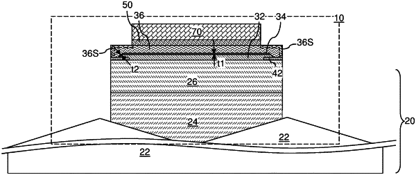
1. A method of forming a light emitting diode (LED), comprising:
forming n-doped semiconductor material layer;
forming an active region including an optically active compound semiconductor layer stack configured to emit light on the n-doped semiconductor material layer;
forming a p-doped semiconductor material layer on the active region;
deactivating a physically exposed portion of the p-doped semiconductor material layer with a plasma treatment to form an inactive region while an electrically active region remains in the p-doped semiconductor material that is not subjected to the plasma during the plasma treatment;
forming an anode contact on the p-doped semiconductor material layer;
forming a reflector overlying and electrically connected to the anode contact; and
forming a device-side bonding pad layer on the reflector,
wherein an area of an interface between the electrically active region and the anode contact is equal to an area which during LED operation produces a current density in a range from 0.90 times a peak external quantum efficiency of the LED to the peak external quantum efficiency of the LED.
|