US 11,908,968 B2
Optoelectronic device
Romain Coffy, Voiron (FR); Remi Brechignac, Grenoble (FR); and Jean-Michel Riviere, Froges (FR)
Assigned to STMicroelectronics (Grenoble 2) SAS, Grenoble (FR)
Filed by STMicroelectronics (Grenoble 2) SAS, Grenoble (FR)
Filed on Jun. 13, 2022, as Appl. No. 17/838,929.
Application 17/838,929 is a division of application No. 17/071,694, filed on Oct. 15, 2020, granted, now 11,387,381.
Claims priority of application No. 1912261 (FR), filed on Oct. 31, 2019.
Prior Publication US 2022/0310869 A1, Sep. 29, 2022
Int. Cl. H01L 31/16 (2006.01); H01L 23/00 (2006.01)
CPC H01L 31/16 (2013.01) [H01L 24/73 (2013.01); H01L 2224/73265 (2013.01)] 15 Claims
OG exemplary drawing
 
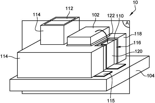
1. A method of manufacturing an optoelectronic device, comprising:
encapsulating an emitter of light rays in a first transparent block;
forming a layer at least partially covering an upper surface and a side surface of the first transparent block, said layer being opaque to wavelengths of light rays emitted by the emitter;
mounting a receiver of light rays to said layer at the upper surface of the first transparent block.