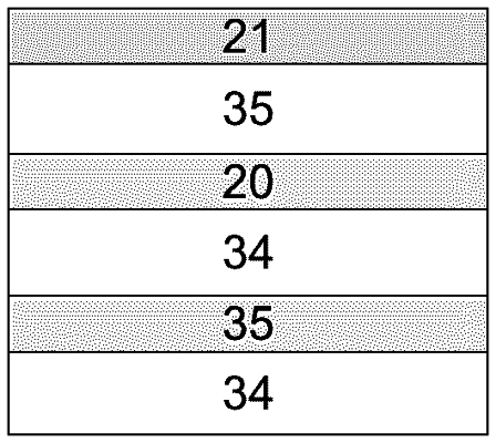
| CPC H01L 31/0376 (2013.01) [H01L 31/02165 (2013.01); H01L 31/02168 (2013.01); Y02E 10/52 (2013.01)] | 17 Claims |

|
1. A photovoltaic device, comprising:
an active photovoltaic device region comprising alternating layers of different amorphous photovoltaic materials,
a first band-stop filter structure on the active photovoltaic device region;
an intermediate photovoltaic layer on the first band-stop filter structure;
a second band-stop filter structure on the first band-stop filter structure intermediate photovoltaic layer such that the intermediate photovoltaic layer is interposed between the first and second first and second band-stop filter structures,
wherein each of the first and second band-stop filter structures comprise:
alternating layers of dielectric materials having a stopband extending from a lower limiting angular frequency ωmin≥0 to an upper limiting angular frequency ωmax, wherein ωmax>ωmin, the first band-stop filter structure on the active photovoltaic device region such that the alternating layers of different amorphous photovoltaic materials are arranged completely beneath the first and second band-stop filter structures and such that the at least one of the first and second band-stop filter structure is arranged in the photovoltaic device relative to the alternating layers of different amorphous photovoltaic materials in order to block electromagnetic radiations reaching portions of the alternating layers of different amorphous photovoltaic materials with angular frequencies of ω* in the stopband, so that ωmin<ω*<ωmax;
wherein said angular frequencies ω* correspond to blocked electronic excitations ℏω* from valence band tail (VBT) states of each amorphous photovoltaic material included in the alternating layers of different amorphous photovoltaic materials to conduction band tail (CBT) states of each amorphous photovoltaic material included in the alternating layers of different amorphous photovoltaic materials;
wherein the angular frequencies of the blocked electromagnetic radiations are the same as the angular frequencies that correspond to the blocked electronic excitations;
wherein light at angular frequencies ω* cause light-induced degradation of the photovoltaic device,
wherein ωmax is based on an Urbach energy component EUC of a conduction band tail region,
wherein ωmin is based on an Urbach energy component EUV of a valence band tail region, and
wherein the photovoltaic device permits electromagnetic radiations reaching portions of a given amorphous photovoltaic material included in the alternating layers of different amorphous photovoltaic materials with angular frequencies of ω* in the stopband, where the electromagnetic radiations have angular frequencies that are >ωmax or <ωmin.
|