| CPC H01L 29/78642 (2013.01) [H01L 29/41741 (2013.01); H01L 29/66666 (2013.01)] | 8 Claims |
|
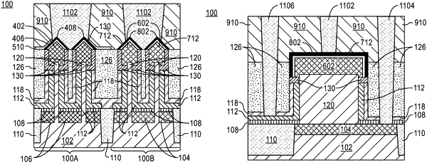
1. A semiconductor structure, comprising:
a channel fin extending perpendicularly from a semiconductor substrate;
a top source/drain region in contact with a top portion of the channel fin,
the top source/drain region including a bottom portion abutted by a first side of a top spacer and a top portion extending outwards from the top spacer,
a second side of the top spacer, opposing the first side, being in contact with a first interlevel dielectric layer;
a bottom source/drain region disposed above the semiconductor substrate and in contact with opposite sidewalls of a bottom portion of the channel fin;
a metal gate stack in contact with a central portion of the channel fin, the metal gate stack being separated from the top source/drain region by the top spacer and from the bottom source/drain region by a bottom spacer;
a silicide layer disposed above and in direct contact with opposite sidewalls of the top portion of the top source/drain region; and
a nitride layer disposed above and in direct contact with an uppermost surface of the silicide layer,
a topmost surface of the top spacer being in contact with opposing ends of the silicide layer and the nitride layer.
|