| CPC H01L 29/7855 (2013.01) [H01L 21/823431 (2013.01); H01L 29/0673 (2013.01); H01L 29/1033 (2013.01); H01L 29/42392 (2013.01); H01L 29/66439 (2013.01); H01L 29/66545 (2013.01); H01L 29/66818 (2013.01); H01L 29/775 (2013.01); H01L 29/78696 (2013.01); H01L 29/045 (2013.01); H01L 2029/7858 (2013.01)] | 20 Claims |

|
1. A semiconductor device, comprising:
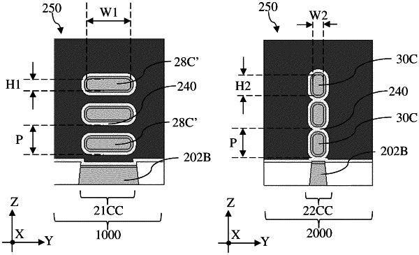
a first transistor comprising:
first nanostructures disposed one over another and extending between a first source/drain feature and a second source/drain feature along a first direction, and
a first gate structure wrapping around each of the first nanostructures; and
a second transistor comprising:
second nanostructures disposed one over another and extending between a third source/drain feature and a fourth source/drain feature along the first direction, and
a second gate structure disposed over the second nanostructures,
wherein the first source/drain feature comprises a first width along a second direction perpendicular to the first direction,
wherein the third source/drain feature comprises a second width along the second direction,
wherein the first width is greater than the second width,
wherein the second gate structure comprises a gate dielectric layer and the gate dielectric layer disposed over two adjacent ones of the second nanostructures merge.
|