US 11,908,939 B2
Method of making a FinFET device including a step of recessing a subset of the fins
Chia Tai Lin, Taichung (TW); Yih-Ann Lin, Jhudong Township (TW); An-Shen Chang, Jubei (TW); Ryan Chen, Chiayi (TW); and Chao-Cheng Chen, Hsin-Chu (TW)
Assigned to TAIWAN SEMICONDUCTOR MANUFACTURING COMPANY, LTD., Hsin-Chu (TW)
Filed by Taiwan Semiconductor Manufacturing Company, Ltd., Hsin-Chu (TW)
Filed on Aug. 16, 2021, as Appl. No. 17/403,318.
Application 14/882,144 is a division of application No. 14/162,598, filed on Jan. 23, 2014, granted, now 9,190,496, issued on Nov. 17, 2015.
Application 17/403,318 is a continuation of application No. 16/876,753, filed on May 18, 2020, granted, now 11,094,825.
Application 16/876,753 is a continuation of application No. 15/817,648, filed on Nov. 20, 2017, granted, now 10,658,509, issued on May 19, 2020.
Application 15/817,648 is a continuation of application No. 14/882,144, filed on Oct. 13, 2015, granted, now 9,825,173, issued on Nov. 21, 2017.
Prior Publication US 2021/0376141 A1, Dec. 2, 2021
Int. Cl. H01L 29/78 (2006.01); H01L 29/66 (2006.01); H01L 29/40 (2006.01); H01L 21/8234 (2006.01); H01L 21/84 (2006.01)
CPC H01L 29/785 (2013.01) [H01L 21/823431 (2013.01); H01L 21/845 (2013.01); H01L 29/401 (2013.01); H01L 29/66795 (2013.01)] 20 Claims
OG exemplary drawing
 
1. A method comprising:
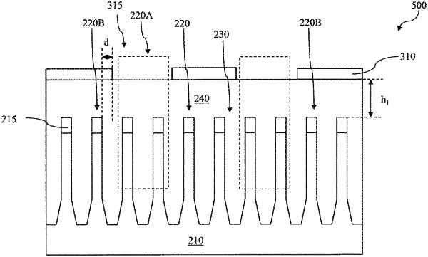
forming fins over a substrate;
forming a dielectric layer over the fins;
removing a first portion of the dielectric layer to form a trench within the dielectric layer, wherein a subset of the fins is exposed in the trench, wherein at least one fin from the subset of the fins includes a semiconductor material layer that is exposed in the trench after the removing of the first portion of the dielectric layer;
removing a second portion of the dielectric layer to enlarge the trench; and
recessing the subset of fins in the enlarged trench.