| CPC H01L 29/7846 (2013.01) [H01L 29/66553 (2013.01); H01L 29/785 (2013.01); H01L 2029/7858 (2013.01); H10B 10/12 (2023.02)] | 7 Claims |
|
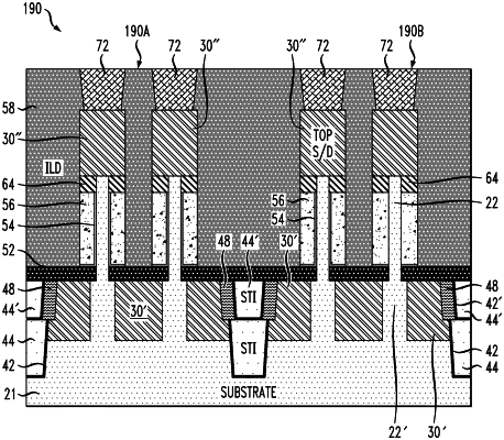
1. A semiconductor structure comprising:
a semiconductor substrate;
one or more active regions on the semiconductor substrate, each of the one or more active regions comprising:
a plurality of vertical transport field-effect transistors extending vertically with respect to the semiconductor substrate;
merged, bottom source/drain regions for the plurality of the vertical transport field-effect transistors; and
a peripheral side wall extending downwardly from a top surface of the merged, bottom source/drain regions and comprising a metal silicide contact wrapping around the merged bottom source/drain regions; and
shallow trench isolation regions surrounding, respectively, each of the one or more active regions and wherein the shallow trench isolation regions comprise:
a first dielectric liner adjoining the substrate and bottom portions of the peripheral side walls of the active regions;
a first layer of STI dielectric material within the first dielectric liner;
a second dielectric liner on a top surface of the first layer of STI dielectric material and adjoining the metal silicide contact; and
a second layer of STI dielectric material within the second dielectric liner.
|