| CPC H01L 29/7786 (2013.01) [H01L 29/2003 (2013.01); H01L 29/205 (2013.01); H01L 29/401 (2013.01); H01L 29/42316 (2013.01); H01L 29/66462 (2013.01)] | 16 Claims |
|
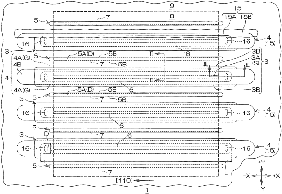
1. A nitride semiconductor device comprising: a first nitride semiconductor layer that constitutes an electron transit layer;
a second nitride semiconductor layer that is formed on the first nitride semiconductor layer and constitutes an electron supply layer;
a nitride semiconductor gate layer that is disposed on the second nitride semiconductor layer, has a ridge portion at least at a portion thereof, and contains an acceptor type impurity;
a gate electrode that is disposed at least on the ridge portion of the nitride semiconductor gate layer;
a source electrode that is disposed on the second nitride semiconductor layer and has a source principal electrode portion parallel to the ridge portion; and
a drain electrode that is disposed on the second nitride semiconductor layer and has a drain principal electrode portion parallel to the ridge portion; and
wherein a length direction of the ridge portion is a [110] direction of a semiconductor crystal structure that constitutes the second nitride semiconductor layer.
|