| CPC H01L 29/66545 (2013.01) [H01L 21/30621 (2013.01); H01L 21/823431 (2013.01); H01L 29/66795 (2013.01); H01L 29/7856 (2013.01); H01L 2029/7858 (2013.01)] | 20 Claims |
|
1. A semiconductor device comprising:
a fin protruding above a substrate;
isolation regions on opposing sides of the fin;
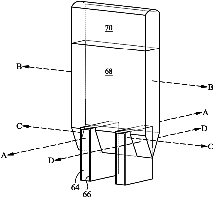
a gate structure over the fin, wherein the gate structure comprises a gate dielectric layer and a gate electrode over the gate dielectric layer;
gate spacers along opposing sidewalls of the gate structure, wherein a first width of a lower portion of the gate structure proximate to the isolation regions, measured between the gate spacers, decreases as the lower portion of the gate structure extends toward the isolation regions; and
a gate fill material along sidewalls of the lower portion of the gate structure, wherein the gate fill material is between the gate structure and the gate spacers, wherein the gate structure extends into the isolation regions, and is closer to the substrate than a lowest surface of the gate fill material facing the isolation regions.
|