| CPC H01L 29/66484 (2013.01) [H01L 21/823418 (2013.01); H01L 21/823431 (2013.01); H01L 29/66553 (2013.01); H01L 29/66795 (2013.01); H01L 29/7831 (2013.01); H01L 29/7848 (2013.01)] | 20 Claims |
|
1. A method of manufacturing a semiconductor device, comprising:
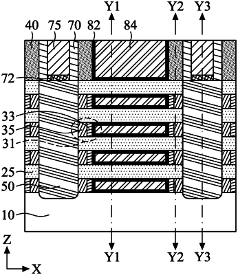
forming a fin structure in which first semiconductor layers and second semiconductor layers are alternatingly stacked;
forming a sacrificial gate structure over the fin structure;
etching a source/drain (S/D) region of the fin structure, which is not covered by the sacrificial gate structure, thereby forming an S/D space;
laterally etching the first semiconductor layers through the S/D space, thereby forming recesses;
forming a first insulating layer, in the recesses, on the etched first semiconductor layers;
after the first insulating layer is formed, forming a second insulating layer, in the recesses, on the first insulating layer, wherein a dielectric constant of the second insulating layer is less than that of the first insulating layer; and
after the second insulating layer is formed, forming an S/D epitaxial layer in the S/D space, wherein the second insulating layer is in contact with the S/D epitaxial layer, and wherein the second insulating layer separates the first insulating layer from physically contacting the S/D epitaxial layer.
|