| CPC H01L 29/41775 (2013.01) [H01L 29/401 (2013.01); H01L 29/41733 (2013.01); H01L 29/4236 (2013.01); H01L 29/42384 (2013.01); H01L 29/458 (2013.01); H01L 29/4908 (2013.01)] | 20 Claims |
|
1. A semiconductor device comprising:
an active region;
an epitaxial source/drain in and extending above the active region;
a first dielectric layer over a portion of the active region;
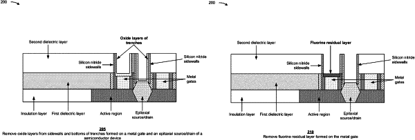
a first metal gate and a second metal gate in the first dielectric layer;
a second dielectric layer over the first dielectric layer and the second metal gate;
a titanium layer on the first metal gate and on the epitaxial source/drain,
wherein the titanium layer is on the first metal gate without an intervening fluorine residual layer,
wherein the titanium layer is on the epitaxial source/drain with an intervening silicide layer;
a first metal layer on top of the titanium layer on the first metal gate;
a second metal layer on top of the titanium layer on the epitaxial source/drain;
a third dielectric layer on the second dielectric layer;
a first via, in the third dielectric layer, filled with a material;
a second via, in the third dielectric layer, filled with the material;
a metal layer on the third dielectric layer, the first via, and the second via; and
a fourth dielectric layer on portions of the metal layer.
|