| CPC H01L 29/417 (2013.01) [H01L 29/41741 (2013.01); H01L 29/6609 (2013.01); H01L 29/2003 (2013.01); H01L 29/205 (2013.01); H01L 29/7788 (2013.01); H01L 29/868 (2013.01)] | 20 Claims |
|
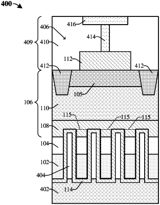
1. A method for forming a semiconductor structure, comprising:
forming a buffer layer over a substrate;
forming an active layer on the buffer layer;
forming a top electrode on the active layer; and
performing an etch process on the buffer layer and the substrate to define a plurality of pillar structures, wherein the plurality of pillar structures comprise a first pillar structure laterally offset from a second pillar structure, wherein at least portions of the first and second pillar structures are spaced laterally between sidewalls of the top electrode, wherein the etch process is performed while the top electrode is disposed on the active layer.
|