| CPC H01L 29/401 (2013.01) [H01L 29/0665 (2013.01); H01L 29/42392 (2013.01); H01L 29/66484 (2013.01); H01L 29/66545 (2013.01)] | 20 Claims |
|
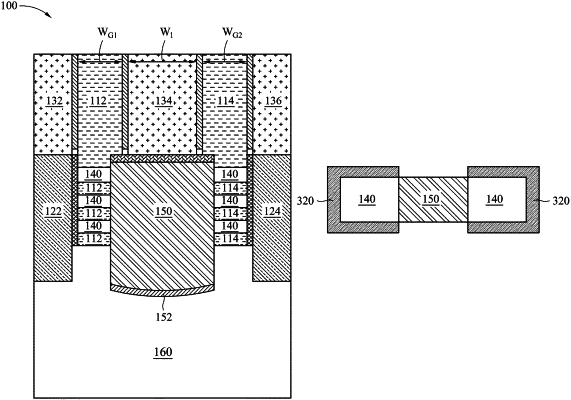
1. A method of fabricating a semiconductor structure, comprising:
removing a portion of an active channel structure to form a recess;
filling the recess with dielectric material;
forming a cladding layer adjacent the active channel structure but not adjacent the dielectric material;
forming a gate structure around the active channel structure, wherein the gate structure comprises an active gate structure;
forming a dummy gate structure around the active channel structure; and
removing the dummy gate structure before forming the active gate structure.
|