US 11,908,900 B2
Passivation layer for epitaxial semiconductor process
Yin-Kai Liao, Taipei (TW); Sin-Yi Jiang, Hsinchu (TW); Hsiang-Lin Chen, Hsinchu (TW); Yi-Shin Chu, Hsinchu (TW); Po-Chun Liu, Hsinchu (TW); Kuan-Chieh Huang, Hsinchu (TW); Jyh-Ming Hung, Dacun Township (TW); and Jen-Cheng Liu, Hsin-Chu (TW)
Assigned to Taiwan Semiconductor Manufacturing Company, Ltd., Hsinchu (TW)
Filed by Taiwan Semiconductor Manufacturing Company, Ltd., Hsin-Chu (TW)
Filed on Jul. 21, 2022, as Appl. No. 17/869,885.
Application 17/869,885 is a division of application No. 17/036,287, filed on Sep. 29, 2020, granted, now 11,508,817.
Claims priority of provisional application 63/030,980, filed on May 28, 2020.
Prior Publication US 2022/0367638 A1, Nov. 17, 2022
Int. Cl. H01L 29/10 (2006.01); H01L 29/167 (2006.01); H01L 29/49 (2006.01); H01L 29/66 (2006.01)
CPC H01L 29/1087 (2013.01) [H01L 29/167 (2013.01); H01L 29/4933 (2013.01); H01L 29/6659 (2013.01)] 20 Claims
OG exemplary drawing
 
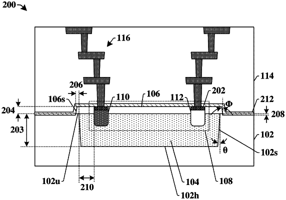
1. An integrated chip, comprising:
a substrate comprising a first semiconductor material;
a second semiconductor material disposed on the first semiconductor material, wherein the second semiconductor material is a group IV semiconductor or a group III-V compound semiconductor;
a passivation layer disposed on the second semiconductor material, wherein the passivation layer comprises the first semiconductor material; and
a first doped region and a second doped region extending through the passivation layer and into the second semiconductor material, wherein the first doped region has a first doping type and the second doped region has a second doping type that is different than the first doping type.