| CPC H01L 29/0821 (2013.01) [H01L 29/735 (2013.01)] | 18 Claims |
|
1. An electrostatic discharge protection device, comprising:
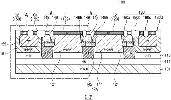
an emitter region having a first conductivity-type on a semiconductor substrate;
a base region having a second conductivity-type opposite to the first conductivity-type, and surrounding the emitter region on the semiconductor substrate;
a first collector region having the first conductivity-type surrounding the base region on the semiconductor substrate;
a second collector region having the first conductivity-type surrounding the first collector region on the semiconductor substrate;
a second conductivity-type drift region surrounded by the base region, wherein the second conductivity-type drift region is between the emitter region and the semiconductor substrate, and extends toward the semiconductor substrate deeper than the base region;
a second conductivity-type well region between the base region and the semiconductor substrate, and having a junction interface with the second conductivity-type drift region; and
a plurality of isolation portions between the emitter region and the base region, between the base region and the first collector region, and between the first collector region and the second collector region, respectively, wherein:
the second conductivity-type well region comprises a second conductivity-type deep well having the junction interface and having a first impurity concentration, and a second conductivity-type shallow well surrounding the base region in the second conductivity-type deep well and having a second impurity concentration that is higher than the first impurity concentration; and
the base region comprises a high doped concentration region and a second conductivity-type body region within the second conductivity-type shallow well.
|