| CPC H01L 29/0673 (2013.01) [H01L 27/0886 (2013.01); H01L 29/0843 (2013.01); H01L 29/1029 (2013.01); H01L 29/42392 (2013.01); H01L 29/4966 (2013.01); H01L 29/66439 (2013.01); H01L 29/66795 (2013.01); H01L 29/785 (2013.01); H01L 29/7851 (2013.01); H01L 29/78696 (2013.01)] | 20 Claims |
|
1. A semiconductor device comprising:
source and drain regions;
a channel region between the source and drain regions; and
a gate structure over the channel region and comprising:
a gate dielectric over the channel region;
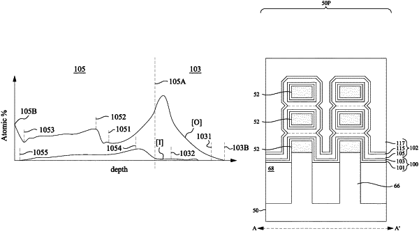
a work function metal layer over the gate dielectric and comprising iodine, wherein the work function metal layer has an oxygen concentration in a range from about 10 at % to about 30 at % throughout the work function metal layer; and
a fill metal over the work function metal layer.
|