US 11,908,885 B2
Semiconductor device structure with magnetic element
Chin-Yu Ku, Hsinchu (TW); Chi-Cheng Chen, Tainan (TW); Hon-Lin Huang, Hsinchu (TW); Wei-Li Huang, Pingtung County (TW); Chun-Yi Wu, Tainan (TW); and Chen-Shien Chen, Zhubei (TW)
Assigned to Taiwan Semiconductor Manufacturing Company, Ltd., Hsinchu (TW)
Filed by Taiwan Semiconductor Manufacturing Company, Ltd., Hsinchu (TW)
Filed on May 9, 2022, as Appl. No. 17/739,487.
Application 17/739,487 is a continuation of application No. 16/907,699, filed on Jun. 22, 2020, granted, now 11,329,124.
Application 16/907,699 is a continuation of application No. 16/260,439, filed on Jan. 29, 2019, granted, now 10,720,487, issued on Jul. 7, 2020.
Claims priority of provisional application 62/691,108, filed on Jun. 28, 2018.
Prior Publication US 2022/0262892 A1, Aug. 18, 2022
Int. Cl. H01L 49/02 (2006.01)
CPC H01L 28/10 (2013.01) 20 Claims
OG exemplary drawing
 
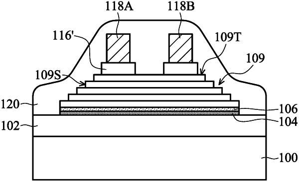
1. A semiconductor device structure, comprising:
a substrate;
a magnetic element over the substrate;
an isolation element over the magnetic element, wherein the magnetic element is wider than the isolation element;
a conductive line over the isolation element;
a second isolation element extending across the magnetic element, wherein the second isolation element partially covers the top surface of the magnetic element and partially covers sidewall surfaces of the magnetic element; and
a second conductive line over the second isolation element.