| CPC H01L 27/156 (2013.01) [G09G 3/32 (2013.01); H01L 33/38 (2013.01); H01L 33/62 (2013.01); H05K 1/189 (2013.01); G09G 2310/0267 (2013.01); H05K 2201/10128 (2013.01)] | 20 Claims |
|
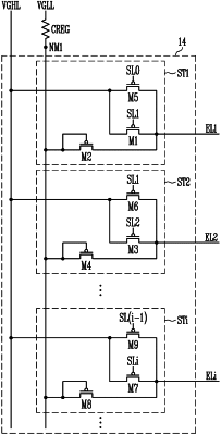
1. A display device comprising:
pixels each connected to at least one of scan lines and at least one of emission lines;
a scan driver providing scan signals to the scan lines; and
an emission driver including stages connected to the emission lines, each of the stages providing an emission signal to a corresponding emission line of the emission lines, a first stage among the stages including:
a first transistor including:
a first electrode connected to a first power source line;
a second electrode connected to a first emission line of the emission lines; and
a gate electrode connected to a first scan line of the scan lines; and
a second transistor including:
a first electrode connected to a first node; and
a second electrode connected to the first emission line.
|