| CPC H01L 27/1463 (2013.01) [H01L 27/1464 (2013.01); H01L 27/14623 (2013.01); H01L 27/14636 (2013.01); H01L 27/14685 (2013.01)] | 20 Claims |
|
1. An image sensor, comprising:
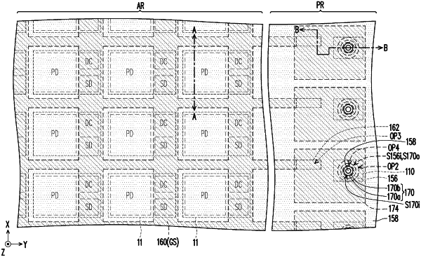
a substrate, having an active region and a peripheral region next to the active region;
a pixel arranged in the active region and comprising a photosensitive region and a circuitry region next to the photosensitive region;
an isolation structure disposed in the substrate at a first side of the substrate surrounding the photosensitive region, wherein the isolation structure comprises a conductive grid and a dielectric structure covering a sidewall of the conductive grid;
a conductive structure disposed in the substrate within the peripheral region, wherein the conductive grid is electrically connected to the conductive structure; and
an isolation disposed in the substrate under the conductive structure at a second side opposite to the first side of the substrate,
wherein the conductive structure is in contact with the isolation and electrically connecting the conductive grid and a conductive component at the first side of the substrate through the isolations.
|