| CPC H01L 27/1248 (2013.01) [G02F 1/133345 (2013.01); G02F 1/136227 (2013.01); H01L 27/1225 (2013.01); H01L 27/124 (2013.01); H01L 27/1255 (2013.01); H01L 27/156 (2013.01); H10K 59/124 (2023.02); H10K 59/1213 (2023.02); H10K 2102/311 (2023.02)] | 12 Claims |
|
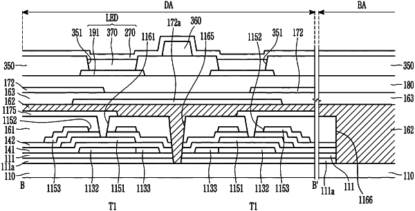
1. A display device comprising:
a substrate;
a semiconductor layer disposed on the substrate;
a first gate insulating layer disposed on the semiconductor layer;
a gate electrode positioned on the first gate insulating layer;
a second gate insulating layer disposed on the gate electrode;
a first storage electrode positioned on the second gate insulating layer;
a first interlayer insulating layer disposed on the first storage electrode to have an opening surrounding the semiconductor layer, the gate electrode, and the first storage electrode;
a second interlayer insulating layer disposed on the first interlayer insulating layer and filling the opening; and
a data line and a driving voltage line positioned on the second interlayer insulating layer,
wherein the semiconductor layer, the gate electrode, and the first storage electrode are included in a pixel circuit region,
the display device includes a plurality of pixel circuit regions,
the data line and the driving voltage line cross the pixel circuit region, and
a portion of the semiconductor layer is in contact with the second interlayer insulating layer filling the opening.
|