| CPC H01L 27/0924 (2013.01) [H01L 27/0207 (2013.01); H01L 21/02529 (2013.01); H01L 21/02532 (2013.01); H01L 21/823814 (2013.01); H01L 29/0847 (2013.01); H01L 29/165 (2013.01); H01L 29/41783 (2013.01); H01L 29/7848 (2013.01)] | 20 Claims |
|
1. A semiconductor device comprising:
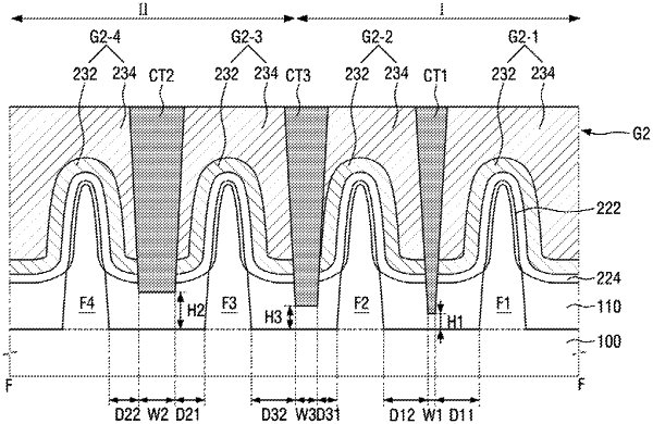
a first active pattern, a second active pattern, a third active pattern, and a fourth active pattern, all of which extend in parallel in a first direction, and are arranged along a second direction intersecting the first direction;
a field insulating film covering a part of side surfaces of the first to fourth active patterns;
a gate electrode provided on the first to fourth active patterns and extending in the second direction;
a gate dielectric film interposed between the first to fourth active patterns and the gate electrode, and between the field insulating film and the gate electrode;
a first cut region that extends from a top surface of the gate electrode into the field insulating film between the first active pattern and the second active pattern to cut the gate electrode and the gate dielectric film; and
a second cut region that extends from the top surface of the gate electrode into the field insulating film between the third active pattern and the fourth active pattern to cut the gate electrode and the gate dielectric film,
wherein a first width of the first cut region in the second direction at the top surface of the gate electrode is different from a second width of the second cut region in the second direction at the top surface of the gate electrode,
wherein a first length of the first cut region from a bottom surface of the first cut region to the top surface of the gate electrode is different from a second length of the second cut region from a bottom surface of the second cut region to the top surface of the gate electrode, and
wherein the first length of the first cut region and the second length of the second cut region are longer than a third length from a top surface of the field insulating film to the top surface of the gate electrode.
|