| CPC H01L 27/0924 (2013.01) [H01L 21/82385 (2013.01); H01L 21/823821 (2013.01); H01L 21/823842 (2013.01); H01L 29/4236 (2013.01); H01L 29/4238 (2013.01); H01L 29/66545 (2013.01); H01L 29/66795 (2013.01); H01L 29/785 (2013.01); H01L 27/092 (2013.01)] | 20 Claims |
|
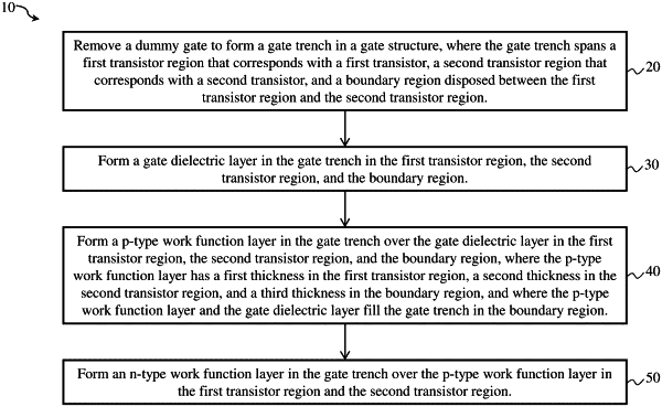
1. A method comprising:
removing a dummy gate to form a gate trench in a gate structure, wherein the gate structure includes a first transistor region that corresponds with a first transistor, a second transistor region that corresponds with a second transistor, and a boundary region disposed between the first transistor region and the second transistor region;
forming a gate dielectric layer in the gate trench in the first transistor region, the second transistor region, and the boundary region;
forming a p-type work function layer in the gate trench over the gate dielectric layer in the first transistor region, the second transistor region, and the boundary region, wherein the p-type work function layer has a first thickness in the first transistor region, a second thickness in the second transistor region, and a third thickness in the boundary region, wherein the p-type work function layer and the gate dielectric layer fill the gate trench in the boundary region; and
forming an n-type work function layer in the gate trench over the p-type work function layer in the first transistor region and the second transistor region.
|