US 11,908,864 B2
Method of manufacturing semiconductor devices and a semiconductor device
Chun-Hung Chen, Hsinchu (TW); Chih-Hung Hsieh, Hsinchu (TW); and Jhon Jhy Liaw, Zhudong Township (TW)
Assigned to Taiwan Semiconductor Manufacturing Company, Ltd., Hsinchu (TW)
Filed by TAIWAN SEMICONDUCTOR MANUFACTURING COMPANY, LTD., Hsinchu (TW)
Filed on Nov. 1, 2021, as Appl. No. 17/516,110.
Application 17/516,110 is a division of application No. 16/019,420, filed on Jun. 26, 2018, granted, now 11,164,746, issued on Nov. 2, 2021.
Prior Publication US 2022/0059351 A1, Feb. 24, 2022
Int. Cl. H01L 27/092 (2006.01); H01L 21/265 (2006.01); H01L 27/088 (2006.01); H01L 21/266 (2006.01); H10B 10/00 (2023.01)
CPC H01L 27/0924 (2013.01) [H01L 21/266 (2013.01); H01L 21/26513 (2013.01); H01L 21/26533 (2013.01); H01L 21/26586 (2013.01); H01L 27/0886 (2013.01); H01L 27/0921 (2013.01); H01L 27/0928 (2013.01); H10B 10/12 (2023.02)] 20 Claims
OG exemplary drawing
 
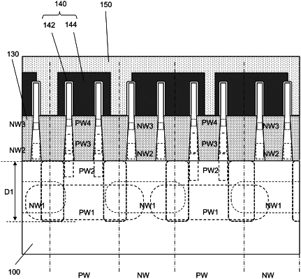
1. A semiconductor device comprising:
a semiconductor substrate;
a first fin structure protruding from the semiconductor substrate;
a second fin structure protruding from the semiconductor substrate; and
a carbon barrier region disposed at a region of the semiconductor substrate between the first fin structure and the second fin structure
wherein the carbon barrier region extends to a bottom of each of the first and second fin structures.