| CPC H01L 27/0924 (2013.01) [H01L 29/66492 (2013.01); H01L 29/7833 (2013.01)] | 13 Claims |
|
1. A transistor device comprising:
a substrate;
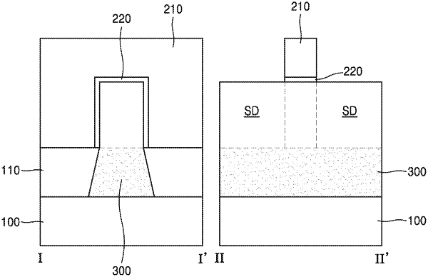
a fin structure extending on the substrate in a direction parallel to a top surface of the substrate;
a source region and a drain region provided at an upper portion of the fin structure;
a constant current generating layer provided at a lower portion of the fin structure;
a gate insulating film provided on both side surfaces and a top surface of the upper portion of the fin structure; and
a gate electrode provided on the gate insulating film,
wherein the gate electrode is provided on the fin structure and between the source region and the drain region,
the substrate and the constant current generating layer have a first conductivity type,
the source region and the drain region have a second conductivity type that is different from the first conductivity type,
the constant current generating layer generates a constant current between the drain region and the substrate, and an electric field is formed between the drain region and the constant current generating layer, and
the constant current is independent from a gate voltage applied to the gate electrode.
|