| CPC H01L 27/0922 (2013.01) | 19 Claims |
|
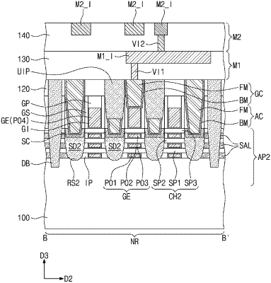
1. A semiconductor device, comprising:
an active pattern on a substrate;
a pair of source/drain patterns on the active pattern;
fence spacers on opposing side surfaces of each of the pair of source/drain patterns;
a channel pattern extending between the pair of source/drain patterns;
a gate electrode crossing the channel pattern and extending in a first direction; and
a gate spacer on a side surface of the gate electrode,
wherein a first thickness of an upper portion of the fence spacers in the first direction is greater than a second thickness of the gate spacer in a second direction crossing the first direction,
wherein the source/drain patterns have a first height, the fence spacers have a second height, and the second height is 50% to 100% of the first height.
|