US 11,908,859 B2
Semiconductor device including transistors sharing gates with structures having reduced parasitic circuit
Yi-Feng Chang, New Taipei (TW); Po-Lin Peng, Taoyuan (TW); and Jam-Wem Lee, Hsinchu (TW)
Assigned to TAIWAN SEMICONDUCTOR MANUFACTURING CO., LTD., Hsinchu (TW)
Filed by TAIWAN SEMICONDUCTOR MANUFACTURING CO., LTD., Hsinchu (TW)
Filed on Jan. 7, 2022, as Appl. No. 17/570,872.
Application 16/525,275 is a division of application No. 15/691,725, filed on Aug. 30, 2017, granted, now 10,366,992, issued on Jul. 30, 2019.
Application 17/570,872 is a continuation of application No. 16/525,275, filed on Jul. 29, 2019, granted, now 11,222,893.
Prior Publication US 2022/0130824 A1, Apr. 28, 2022
Int. Cl. H01L 27/02 (2006.01); H01L 27/092 (2006.01); H01L 29/10 (2006.01); H01L 21/8238 (2006.01); H01L 29/06 (2006.01); H01L 29/87 (2006.01)
CPC H01L 27/0921 (2013.01) [H01L 21/823871 (2013.01); H01L 27/0262 (2013.01); H01L 29/0649 (2013.01); H01L 29/1083 (2013.01); H01L 29/87 (2013.01)] 20 Claims
OG exemplary drawing
 
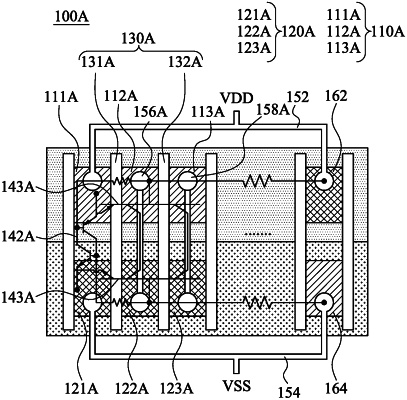
1. A semiconductor device, comprising:
a first region;
a first gate;
a second region disposed opposite to the first region with respect to the first gate;
a first metal contact coupling the first region to the second region;
a third region;
a fourth region disposed opposite to the third region with respect to the first gate;
a second metal contact coupling the third region to the fourth region;
a fifth region disposed between the first gate and the second region, and disconnected from the first metal contact and the second metal contact; and
a sixth region disposed between the first gate and the first region, and disconnected from the first metal contact and the second metal contact.