| CPC H01L 27/0886 (2013.01) [H01L 21/823431 (2013.01); H01L 21/823456 (2013.01); H01L 21/823475 (2013.01); H01L 23/485 (2013.01); H01L 23/5283 (2013.01); H01L 29/42364 (2013.01); H01L 29/42372 (2013.01); H01L 27/0924 (2013.01); H01L 29/7391 (2013.01)] | 20 Claims |
|
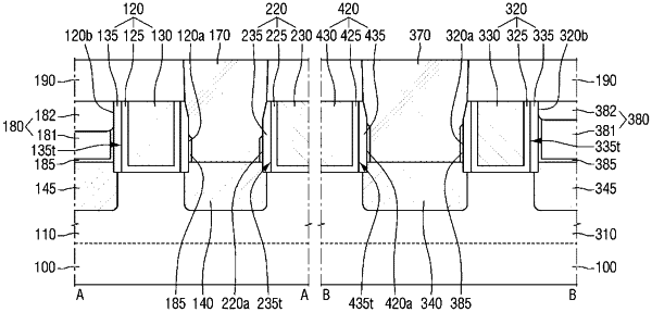
1. A semiconductor device, comprising:
a substrate including a first region and a second region;
a first gate structure and a second gate structure on the substrate of the first region, the first gate structure and the second gate structure being spaced apart by a first distance;
a third gate structure and a fourth gate structure on the substrate of the second region, the third gate structure and the fourth gate structure being spaced apart by a second distance greater than the first distance;
a first liner extending along and contacting a portion of a sidewall of the first gate structure, continuing along and contacting an upper surface of the substrate, and continuing along and contacting a portion of a sidewall of the second gate structure;
a second liner extending along a portion of a sidewall of the third gate structure, the upper surface of the substrate, and a portion of a sidewall of the fourth gate structure;
a first interlayer insulating film on the first liner and surrounding the sidewall of the first gate structure and the sidewall of the second gate structure;
a second interlayer insulating film on the second liner and surrounding the sidewall of the third gate structure and the sidewall of the fourth gate structure;
a first contact between the first gate structure and the second gate structure and within the first interlayer insulating film, the first contact having a first width; and
a second contact between the third gate structure and the fourth gate structure and within the second interlayer insulating film, the second contact having a second width greater than the first width,
the first width being correlated to a width of an upper surface of the first gate structure, and the second width being correlated to a width of an upper surface of the third gate structure.
|