| CPC H01L 27/0207 (2013.01) [G06F 30/394 (2020.01); H01L 23/5226 (2013.01); H01L 27/11807 (2013.01); H01L 2027/11881 (2013.01)] | 20 Claims |
|
1. An integrated circuit, comprising:
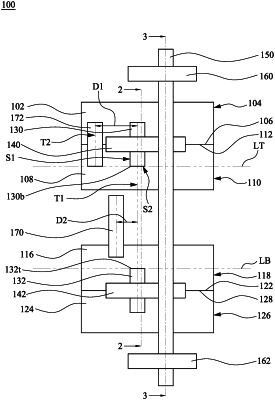
a cell layer including a first cell and a second cell;
a first metal layer over the cell layer and having a first conductive feature, wherein the first conductive feature spans over a boundary between the first and second cells, and has a lengthwise direction along a first direction, and wherein the first metal layer further comprises a third conductive feature, the third conductive feature being misaligned with the first conductive feature along the first direction;
a second metal layer over the first metal layer and having a second conductive feature, wherein the second conductive feature spans over the boundary between the first and second cells, and has a lengthwise direction along a second direction that is perpendicular to the first direction, and wherein a shortest distance between a center line of the first conductive feature and a center line of the third conductive feature along the second direction is less than a width of the first conductive feature; and
a first via between the first metal layer and the second metal layer and connecting the first conductive feature to the second conductive feature.
|