| CPC H01L 27/0207 (2013.01) [H01L 21/28525 (2013.01); H01L 21/28568 (2013.01); H01L 21/823821 (2013.01); H01L 21/823871 (2013.01); H01L 23/5221 (2013.01); H01L 23/5286 (2013.01); H01L 23/53209 (2013.01); H01L 23/53271 (2013.01); H01L 27/0924 (2013.01); H01L 29/41791 (2013.01); H01L 29/4238 (2013.01); H01L 29/42372 (2013.01); H01L 29/42376 (2013.01); H01L 29/66795 (2013.01)] | 20 Claims |
|
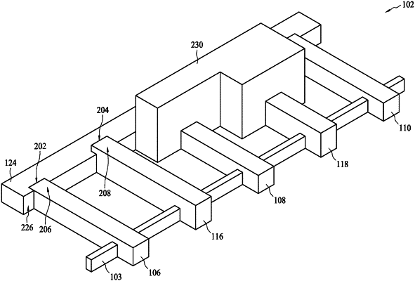
1. A method for forming a semiconductor device, comprising:
forming a fin structure protruding from a substrate of the semiconductor device;
forming a first conductive rail on the substrate, wherein a side of the first conductive rail facing the fin structure has a first recess and a second recess;
forming a first conductive line in a same layer as the first conductive rail by filling a first conductive material into the first recess, wherein the first conductive line extends across the fin structure and wraps a portion of the fin structure; and
forming a second conductive line in the same layer as the first conductive rail by filling a second conductive material into the second recess, wherein the second conductive line extends across the fin structure and contacts another portion of the fin structure.
|