| CPC H01L 25/167 (2013.01) [H01L 33/62 (2013.01); H01L 33/20 (2013.01); H01L 33/44 (2013.01); H01L 33/60 (2013.01)] | 16 Claims |
|
1. A display device comprising:
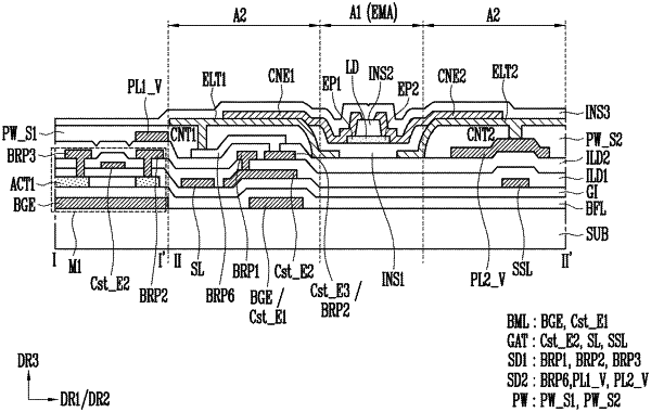
a base layer having a first area and a second area extending at least partially around a periphery of the first area;
conductive patterns in the second area;
an insulating layer covering the conductive patterns in the second area;
a first electrode and a second electrode on the insulating layer, the first electrode and the second electrode being spaced apart from each other in the first area, the first electrode and the second electrode being respectively connected to portions of the conductive patterns through contact openings penetrating the insulating layer;
a plurality of light emitting elements between the first electrode and the second electrode in the first area, the plurality of light emitting elements being connected to the first electrode and the second electrode;
a third electrode on the first electrode and on one end portion of the light emitting elements to contact the first electrode and the one end portion of the light emitting elements; and
a fourth electrode on the second electrode and on the other end portion of the light emitting elements to contact the second electrode and the other end portion of the light emitting elements,
wherein the light emitting elements do not overlap the conductive patterns and the insulating layer.
|