| CPC H01L 25/071 (2013.01) [H01L 23/367 (2013.01); H01L 24/32 (2013.01); H01L 25/50 (2013.01); H01L 2224/32245 (2013.01)] | 20 Claims |
|
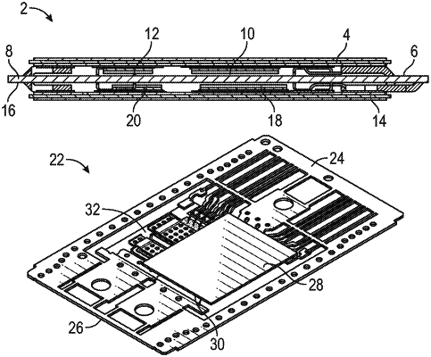
1. A method of forming a semiconductor package, the method comprising:
providing a first panel of first substrates and a second panel of second substrates;
printing a first electrically conductive bonding material on a first side of the first panel of first substrates and a first side of the second panel of second substrates in predetermined locations;
coupling two or more die to each substrate of the first panel of first substrates and to each substrate of the second panel of second substrates at the predetermined locations;
dispensing a second electrically conductive material onto a second side of each of the two or more die;
coupling a clip to each of the two or more die;
electrically coupling the two or more die to each substrate of the first panel of first substrates and to each substrate of the second panel of second substrates;
singulating each of the first panel and the second panel into a plurality of first substrates and a plurality of second substrates, respectively;
dispensing solder onto a plurality of predetermined locations on the first side of each of the plurality of first substrates and each of the plurality of second substrates;
coupling a first substrate of the plurality of first substrates to a first side of a lead frame;
coupling two or more spacers to a first side of the first substrate; and
coupling a first side of a second substrate of the plurality of second substrates to the two or more spacers and to the second side of the lead frame;
wherein the first side of the first substrate and first side of the second substrate are asymmetrically coupled through the two or more spacers.
|