| CPC H01L 25/0657 (2013.01) [H01L 21/56 (2013.01); H01L 25/50 (2013.01); H01L 28/60 (2013.01); H01L 23/3121 (2013.01); H01L 23/3157 (2013.01); H01L 24/08 (2013.01); H01L 24/32 (2013.01); H01L 2224/08145 (2013.01); H01L 2224/32145 (2013.01); H01L 2225/06524 (2013.01); H01L 2225/06548 (2013.01); H01L 2225/06568 (2013.01)] | 20 Claims |
|
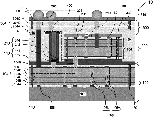
1. A three-dimensional device structure comprising:
a first die comprising a first semiconductor substrate;
a second die disposed on the first die and comprising a second semiconductor substrate;
a dielectric encapsulation (DE) layer disposed on the first die and surrounding the second die;
a redistribution layer structure disposed on the second die and the DE layer; and
deep trench capacitor (DTC) disposed in a trench formed in the DE layer and electrically connected to the first die and the redistribution layer structure, the DTC comprising:
a first conductive layer electrically connected to the first die;
a second conductive layer electrically connected to the redistribution layer structure; and
a first dielectric layer disposed between the first conductive layer and the second conductive layer.
|