| CPC H01L 25/0657 (2013.01) [H01L 21/4857 (2013.01); H01L 21/565 (2013.01); H01L 21/568 (2013.01); H01L 21/6835 (2013.01); H01L 21/76898 (2013.01); H01L 23/3128 (2013.01); H01L 23/481 (2013.01); H01L 23/5383 (2013.01); H01L 23/5386 (2013.01); H01L 23/5389 (2013.01); H01L 23/544 (2013.01); H01L 24/08 (2013.01); H01L 24/80 (2013.01); H01L 25/105 (2013.01); H01L 25/50 (2013.01); H01L 2221/68372 (2013.01); H01L 2223/54426 (2013.01); H01L 2224/08145 (2013.01); H01L 2224/80895 (2013.01); H01L 2224/80896 (2013.01); H01L 2225/0651 (2013.01); H01L 2225/06541 (2013.01); H01L 2225/06568 (2013.01); H01L 2225/06586 (2013.01); H01L 2225/06593 (2013.01); H01L 2225/1035 (2013.01); H01L 2225/1058 (2013.01); H01L 2225/1082 (2013.01)] | 20 Claims |
|
1. A method of forming a semiconductor package, comprising:
bonding a first die to a second die, wherein the first die comprises a plurality of first bonding pads, wherein the second die comprises a plurality of second bonding pads bonded to corresponding ones the plurality of first bonding pads, wherein the second die comprises a plurality of through vias electrically connected to corresponding ones of the plurality of second bonding pads;
forming an encapsulating material over the first die, wherein the encapsulating material laterally encapsulates the second die;
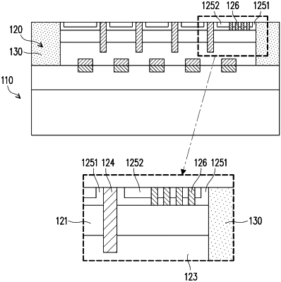
after bonding the first die to the second die, forming a plurality of alignment marks on the second die, wherein a pitch between adjacent two alignment marks of the plurality of alignment marks is different from a pitch between adjacent two through vias of the plurality of through vias; and
forming a redistribution structure over the second die and the encapsulating material.
|