| CPC H01L 25/0655 (2013.01) [H01L 21/4853 (2013.01); H01L 21/4882 (2013.01); H01L 21/54 (2013.01); H01L 23/3142 (2013.01); H01L 23/3178 (2013.01); H01L 23/49811 (2013.01); H01L 25/0652 (2013.01); H01L 25/50 (2013.01); H01L 21/563 (2013.01); H01L 23/3128 (2013.01); H01L 23/36 (2013.01); H01L 23/49816 (2013.01); H01L 23/49827 (2013.01); H01L 2224/0401 (2013.01); H01L 2224/1403 (2013.01); H01L 2224/14181 (2013.01); H01L 2224/16225 (2013.01); H01L 2224/16227 (2013.01); H01L 2224/17181 (2013.01); H01L 2224/32145 (2013.01); H01L 2224/32225 (2013.01); H01L 2224/73204 (2013.01); H01L 2224/73253 (2013.01); H01L 2224/92125 (2013.01); H01L 2225/06513 (2013.01); H01L 2225/06541 (2013.01); H01L 2924/157 (2013.01); H01L 2924/15162 (2013.01); H01L 2924/15311 (2013.01); H01L 2924/15787 (2013.01); H01L 2924/15788 (2013.01); H01L 2924/18161 (2013.01); H01L 2924/3511 (2013.01)] | 20 Claims |
|
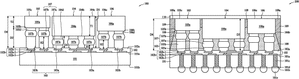
1. A method of manufacturing a semiconductor structure, comprising:
providing a substrate;
disposing a first conductive pillar, a second conductive pillar and a third conductive pillar over the substrate, the first conductive pillar comprising a first height, the second conductive pillar comprising a second height, and the third conductive pillar comprising a third height different from the first height and the second height;
disposing a first die over the first conductive pillar, the first die comprising a first surface distal to the substrate;
disposing a second die over the second conductive pillar, the second die comprising a second surface distal to the substrate, wherein the first surface of the first die and the second surface of the second die are at substantially same level; and
disposing an underfill material over the substrate, wherein the underfill material encapsulates the first conductive pillar, the second conductive pillar and the third conductive pillar.
|
|
12. A method of manufacturing a semiconductor structure, comprising:
providing a substrate including a redistribution layer (RDL) disposed over the substrate;
disposing a first conductive pillar, a second conductive pillar and a third conductive pillar over the substrate;
disposing a first die over the first conductive pillar;
disposing a second die over the second conductive pillar; and
disposing a third die over the third conductive pillar,
wherein a third height of the third conductive pillar is different from a first height of the first conductive pillar and a second height of the second conductive pillar, and a first surface of the first die, a second surface of the second die and a third surface of the third die are at substantially same level,
wherein the first die comprises a first thickness, the second die comprises a second thickness, and the third die comprises a third thickness different from the first thickness and the second thickness.
|
|
17. A method of manufacturing a semiconductor structure, comprising:
providing a substrate;
forming a first conductive pillar, a second conductive pillar and a third conductive pillar over the substrate, the first conductive pillar comprising a first height, the second conductive pillar comprising a second height, and the third conductive pillar comprising a third height different from the first height and the second height;
disposing a first die over the first conductive pillar, the first die comprising a first surface distal to the substrate;
disposing a second die over the second conductive pillar, the second die comprising a second surface distal to the substrate;
disposing a third die over the third conductive pillar, the third die comprising a third surface distal to the substrate;
disposing an underfill material encapsulating the first conductive pillar, the second conductive pillar, and the third conductive pillar;
disposing a molding over the substrate, the molding comprising a top surface; and
disposing a heat dissipation means over the molding,
wherein the first surface of the first die, the second surface of the second die, the third surface of the third die and the top surface of the molding are at substantially same level, and
wherein a distance between the first conductive pillar and the heat dissipation means is greater than a distance between the second conductive pillar and the heat dissipation means.
|