| CPC H01L 24/97 (2013.01) [H01L 21/52 (2013.01); H01L 24/08 (2013.01); H01L 2224/08235 (2013.01)] | 14 Claims |
|
1. A process for collectively bending microelectronic components comprising the following steps:
producing a microelectronic structure, comprising a microelectronic substrate, having an upper face and an opposite lower face, comprising a plurality of microelectronic components, each of the plurality of microelectronic components comprises lower conductive pads located on the opposite lower face and intended to allow the plurality of microelectronic components to be connected electrically;
providing a shaping carrier having an upper face and an opposite lower face, wherein the upper face comprising a plurality of curved surfaces;
depositing an adhesive lower layer having a thickness larger than the thickness of the lower conductive pads, so as: either to entirely cover the opposite lower face of the microelectronic substrate and the lower conductive pads such that the adhesive lower layer has a free lower face that is continuous and therefore not passed right through by the lower conductive pads which would otherwise protrude from the adhesive lower layer; or to cover the plurality of curved surfaces;
dicing at least the microelectronic substrate to singulate the plurality of microelectronic components; then
transferring the plurality of microelectronic components to the shaping carrier; then
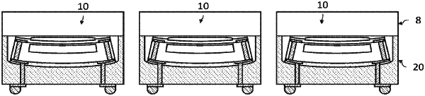
bending the plurality of microelectronic components, the adhesive lower layer then making contact with the lower face of the plurality of microelectronic components and with a corresponding curved surface, thus preventing the lower conductive pads from making contact with the plurality of curved surfaces; then
producing conductive vias that extend through the shaping carrier and the adhesive lower layer from the opposite lower face of the shaping carrier, in order to emerge onto the lower conductive pads.
|