| CPC H01L 24/48 (2013.01) [H01L 23/49822 (2013.01); H01L 24/29 (2013.01); H01L 24/32 (2013.01); H01L 24/37 (2013.01); H01L 24/41 (2013.01); H01L 24/45 (2013.01); H01L 24/73 (2013.01); H01L 25/0655 (2013.01); H01L 2224/29111 (2013.01); H01L 2224/29139 (2013.01); H01L 2224/29147 (2013.01); H01L 2224/32225 (2013.01); H01L 2224/3701 (2013.01); H01L 2224/404 (2013.01); H01L 2224/411 (2013.01); H01L 2224/4516 (2013.01); H01L 2224/45147 (2013.01); H01L 2224/48091 (2013.01); H01L 2224/48225 (2013.01); H01L 2224/48491 (2013.01); H01L 2224/73265 (2013.01); H01L 2924/35 (2013.01)] | 20 Claims |
|
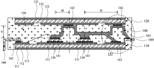
1. A semiconductor package comprising:
a first substrate comprising a specific metal pattern formed thereon to enable electrical connection;
a second substrate facing the first substrate which is spaced apart from the first substrate and comprises a specific metal pattern formed thereon to enable electrical connection;
a first semiconductor chip bonded to an upper surface of the first substrate;
a second semiconductor chip bonded to the upper surface of the first substrate;
a metal bridge which is bent in a specific form to have elasticity, wherein the metal bridge comprises:
a first contact portion bonded to an upper surface of the first semiconductor chip by using a first conductive adhesive;
a second contact portion bonded to a lower surface of the second substrate by using a second conductive adhesive; and
a third contact portion bonded to an upper surface of the second semiconductor chip by using a third conductive adhesive;
a package housing which covers at least a part of the first and second semiconductor chips and the metal bridge; and
at least one terminal lead which is electrically connected to the first substrate, the second substrate, or the metal bridge and is exposed to the outside of the package housing,
wherein a first horizontal bond distance between a first center of the first conductive adhesive and a second center of the second conductive adhesive is 0.5 mm through 7 mm and a vertical bond distance between the first and second conductive adhesives is 0.1 mm through 5 mm,
wherein the second center of the second conductive adhesive is horizontally positioned between the first center of the first conductive adhesive and a third center of the third conductive adhesive.
|