| CPC H01L 24/46 (2013.01) [H01L 24/05 (2013.01); H01L 2924/1423 (2013.01)] | 37 Claims |
|
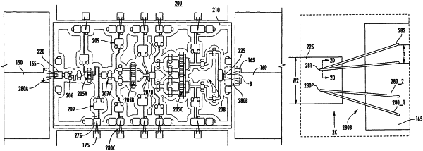
1. A packaged semiconductor device comprising:
a first bond wire comprising a first end and a second end; and
a second bond wire comprising a first end and a second end, wherein the first end of the second bond wire is bonded to a surface of the first end of the first bond wire,
wherein the first end of the second bond wire and the first end of the first bond wire comprise respective widths in a horizontal direction or respective thicknesses in a vertical direction that differ from one another, and
wherein an operating frequency of the packaged semiconductor device is between 500 MHz and 75 GHz.
|