| CPC H01L 24/14 (2013.01) [H01L 21/4846 (2013.01); H01L 21/563 (2013.01); H01L 23/498 (2013.01); H01L 24/11 (2013.01); H01L 24/13 (2013.01); H01L 24/25 (2013.01); H01L 24/26 (2013.01); H01L 24/73 (2013.01); H01L 24/83 (2013.01); H01L 2224/11003 (2013.01); H01L 2224/11424 (2013.01); H01L 2224/11464 (2013.01); H01L 2224/11614 (2013.01); H01L 2224/13083 (2013.01); H01L 2224/13144 (2013.01); H01L 2224/13147 (2013.01); H01L 2224/13155 (2013.01); H01L 2224/13164 (2013.01); H01L 2224/14517 (2013.01); H01L 2224/16112 (2013.01); H01L 2224/24996 (2013.01); H01L 2224/2501 (2013.01); H01L 2224/26155 (2013.01); H01L 2224/26175 (2013.01); H01L 2224/27013 (2013.01); H01L 2224/73204 (2013.01); H01L 2224/83051 (2013.01)] | 20 Claims |
|
1. A semiconductor package comprising:
a packaging substrate including:
a plurality of metal routing layers;
a plurality of dielectric layers including a top dielectric layer forming a topmost surface;
a patterned metal contact layer, wherein the patterned metal contact layer includes:
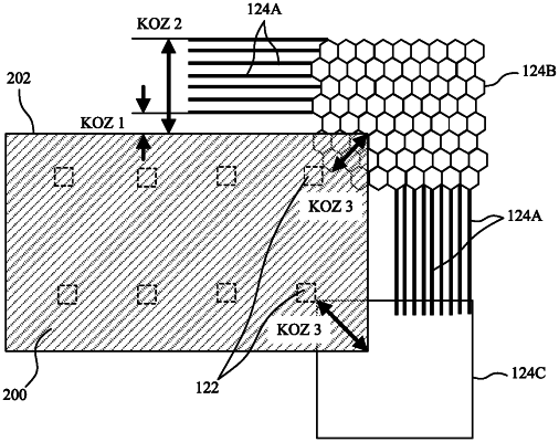
an array of surface mount (SMT) metal bumps in a chip mount area, the array of SMT metal bumps partially embedded within the top dielectric layer and protruding from the topmost surface of the top dielectric layer; and
a metal dam structure laterally surrounding the array of SMT metal bumps in the chip mount area, the metal dam structure partially embedded within the top dielectric layer and protruding from the topmost surface of the top dielectric layer; and
a device bonded to the array of SMT metal bumps;
wherein the metal dam structure forms a first geometric shape adjacent a first edge and a second edge of the device, and a second geometric shape adjacent a corner of the device where the first edge intersects with the second edge.
|