| CPC H01L 24/13 (2013.01) [H01L 24/08 (2013.01); H01L 24/11 (2013.01); H01L 2224/1147 (2013.01); H01L 2224/13144 (2013.01); H01L 2224/13155 (2013.01); H01L 2924/13091 (2013.01)] | 20 Claims |
|
1. A semiconductor device, comprising:
a semiconductor substrate;
a conductive pad over the semiconductor substrate;
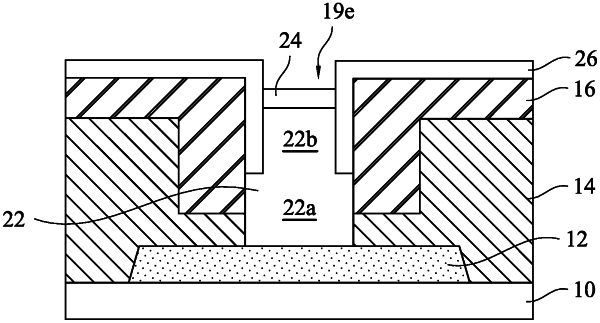
a conductive bump over the conductive pad, wherein the conductive bump has a stepped sidewall structure including a lower sidewall, an upper sidewall laterally offset from the lower sidewall, and an intermediary surface laterally extending from a bottom edge of the upper sidewall to a top edge of the lower sidewall, the conductive bump has a bottom portion over the conductive pad and a top portion over the bottom portion;
a conductive cap over the conductive bump, wherein the bottom portion of the conductive bump is wider than the conductive cap and the top portion of the conductive bump; and
a passivation layer over the semiconductor substrate and laterally surrounding the conductive bump, wherein the passivation layer has a top surface higher than the intermediary surface of the stepped sidewall structure of the conductive bump and lower than a top surface of the conductive cap.
|