| CPC H01L 24/06 (2013.01) [H01L 23/49503 (2013.01); H01L 23/49827 (2013.01); H03K 19/1776 (2013.01)] | 20 Claims |
|
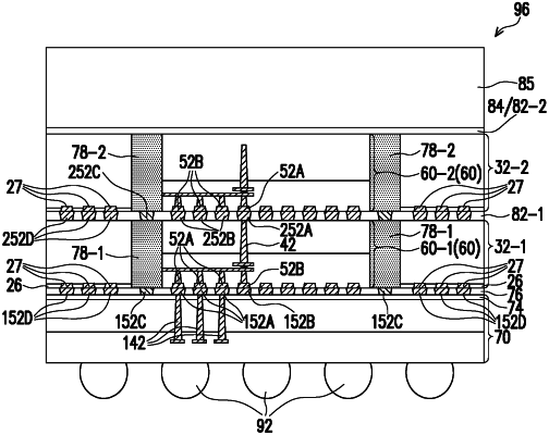
1. A package comprising:
a first die comprising:
a first semiconductor substrate;
a first through-via penetrating through the first semiconductor substrate; and
a first dielectric layer over and contacting the first semiconductor substrate;
a second dielectric layer over the first die;
a first active bond pad in the second dielectric layer, the first active bond pad is over and electrically coupling to the first through-via;
a first dummy bond pad in the second dielectric layer; and
a second die comprising:
a second active bond pad over and bonded to the first active bond pad; and
a dangling bond pad over and bonded to the first dummy bond pad.
|