| CPC H01L 23/53266 (2013.01) [H01L 21/76846 (2013.01)] | 20 Claims |
|
1. A semiconductor structure comprising:
a multi-level interconnect structure;
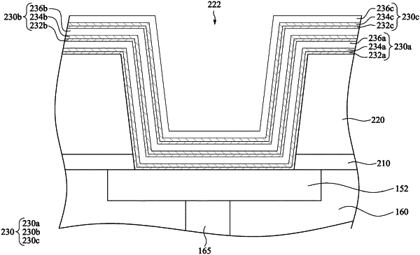
a passivation layer above the multi-level interconnect structure;
a barrier layer lining an inner sidewall of the passivation layer, a top surface of the passivation layer and a top surface of a conductive line of the multi-level interconnect structure, wherein the barrier layer comprises:
a first layer in a nano-crystalline phase;
a second layer above the first layer and in an amorphous phase;
a third layer above the second layer and in a polycrystalline phase; and
a fourth layer above the third layer and in a nano-crystalline phase; and
a pad layer above the barrier layer.
|