| CPC H01L 23/5283 (2013.01) [H01L 21/764 (2013.01); H01L 21/7682 (2013.01); H01L 29/0649 (2013.01); H10B 12/482 (2023.02); H10B 12/485 (2023.02); H10B 12/488 (2023.02); H01L 23/5222 (2013.01); H10B 12/0335 (2023.02); H10B 12/315 (2023.02); H10B 12/34 (2023.02)] | 17 Claims |
|
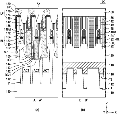
1. An integrated circuit device comprising:
a bit line on a substrate, the bit line comprising a lower conductive layer and an upper conductive layer;
an insulating capping pattern on the bit line; and
a main insulating spacer on a sidewall of the bit line and a sidewall of the insulating capping pattern, the main insulating spacer comprising an extended portion opposite the upper conductive layer, the extended portion protruding toward the upper conductive layer compared to a portion of the main insulating spacer opposite the lower conductive layer,
wherein the extended portion of the main insulating spacer fills an undercut space corresponding to a sidewall of the upper conductive layer and a bottom surface of the insulating capping pattern, and
wherein the extended portion of the main insulating spacer and the portion of the main insulating spacer opposite the lower conductive portion form a continuous portion of a common material.
|
|
10. An integrated circuit device comprising:
a bit line comprising a lower conductive layer and an upper conductive layer on the lower conductive layer in a vertical direction, the lower conductive layer being on a substrate and the upper conductive layer having a width less than a width of the lower conductive layer in a horizontal direction;
an insulating capping pattern on the upper conductive layer in the vertical direction, the insulating capping pattern having a width greater than the width of the upper conductive layer in the horizontal direction; and
a main insulating spacer on a sidewall of the bit line and a sidewall of the insulating capping pattern, the main insulating spacer comprising an extended portion that is convex toward the upper conductive layer,
wherein the width of the upper conductive layer in the horizontal direction varies along the vertical direction.
|
|
14. An integrated circuit device comprising:
a substrate comprising a plurality of active regions apart from each other, the plurality of active regions comprising a first active region and a second active region adjacent to the first active region;
a bit line connected to the first active region and comprising a lower conductive layer and an upper conductive layer stacked on the substrate in a vertical direction;
an insulating capping pattern on the bit line;
a contact plug adjacent to the bit line in a horizontal direction, the contact plug being connected to the second active region; and
a spacer structure between the bit line and the contact plug,
wherein the spacer structure comprises a main insulating spacer comprising an extended portion opposite the upper conductive layer, the extended portion protruding toward the upper conductive layer compared to a portion of the main insulating spacer opposite the lower conductive layer,
wherein the extended portion of the main insulating spacer fills an undercut space corresponding to a sidewall of the upper conductive layer and a bottom surface of the insulating capping pattern, and
wherein the extended portion of the main insulating spacer and the portion of the main insulating spacer opposite the lower conductive portion form a continuous portion of a common material.
|