| CPC H01L 23/5226 (2013.01) [H01L 21/76802 (2013.01); H01L 21/76841 (2013.01); H01L 21/76877 (2013.01); H01L 23/53204 (2013.01)] | 20 Claims |
|
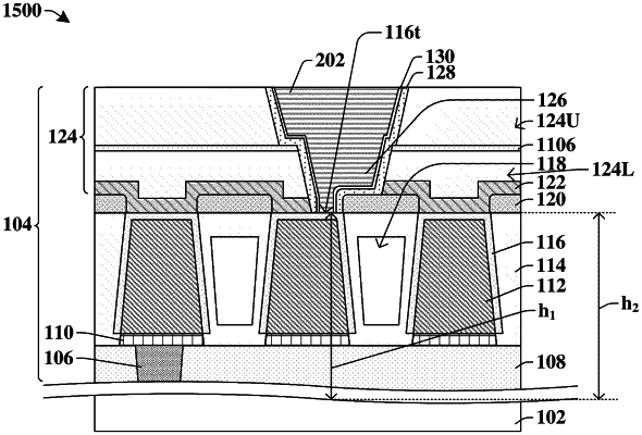
17. A method comprising:
forming an interconnect wire over a substrate;
forming a protection liner on outer surfaces of the interconnect wire;
forming a first interconnect dielectric layer around the interconnect wire;
forming a first etch stop layer selectively on the first interconnect dielectric layer and not on the protection liner; and
forming an interconnect via contacting an upper surface of the protection liner and coupled to the interconnect wire through the protection liner.
|