| CPC H01L 23/5226 (2013.01) [H01L 21/7682 (2013.01); H01L 21/76802 (2013.01); H01L 21/76831 (2013.01); H01L 21/76877 (2013.01); H01L 23/53295 (2013.01)] | 20 Claims |
|
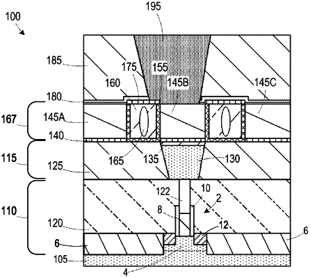
1. A semiconductor device, comprising:
a first conductive feature;
a second conductive feature;
a first dielectric layer positioned between the first conductive feature and the second conductive feature;
an etch stop layer over the first dielectric layer;
a cap layer over the first conductive feature, the second conductive feature, and the etch stop layer, wherein the cap layer is adjacent a first sidewall of the etch stop layer and in direct contact with the first conductive feature; and
a contact overlying a portion of the first dielectric layer positioned between the first conductive feature and the second conductive feature, wherein:
the contact is separated from the portion of the first dielectric layer by the etch stop layer, and
the contact is in direct contact with a top surface of the etch stop layer and electrically coupled to the second conductive feature.
|