| CPC H01L 23/49575 (2013.01) [H01L 23/49513 (2013.01); H01L 23/49562 (2013.01); H01L 24/32 (2013.01); H01L 24/40 (2013.01); H01L 24/41 (2013.01); H01L 24/48 (2013.01); H01L 24/73 (2013.01); H01L 24/83 (2013.01); H01L 24/84 (2013.01); H01L 24/92 (2013.01); H01L 25/074 (2013.01); H01L 25/16 (2013.01); H01L 25/50 (2013.01); H01L 21/561 (2013.01); H01L 21/565 (2013.01); H01L 23/3121 (2013.01); H01L 24/97 (2013.01); H01L 2224/32245 (2013.01); H01L 2224/40145 (2013.01); H01L 2224/40177 (2013.01); H01L 2224/4118 (2013.01); H01L 2224/48091 (2013.01); H01L 2224/48106 (2013.01); H01L 2224/48137 (2013.01); H01L 2224/48247 (2013.01); H01L 2224/73221 (2013.01); H01L 2224/73263 (2013.01); H01L 2224/83815 (2013.01); H01L 2224/84815 (2013.01); H01L 2224/92246 (2013.01); H01L 2924/13091 (2013.01); H01L 2924/1426 (2013.01); H01L 2924/2064 (2013.01)] | 24 Claims |
|
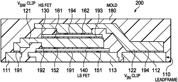
1. A semiconductor package, comprising:
a leadframe including a die pad and a plurality of lead terminals;
a semiconductor device attached on a first side by a die attach material to the die pad,
a first clip on the semiconductor device that is connected to a terminal of the semiconductor device on a second side opposite to the first side providing a first bonded interface, wherein the first clip is connected to at least a first of the plurality of lead terminals;
wherein the first bonded interface includes a first non-metallic protruding surface standoff therein that extends from a surface on the second side of the semiconductor device to physically contact the first clip.
|