| CPC H01L 23/49548 (2013.01) [H01L 21/4828 (2013.01); H01L 21/565 (2013.01); H01L 23/3121 (2013.01); H01L 23/49861 (2013.01); H01L 24/13 (2013.01); H01L 24/16 (2013.01); H01L 24/48 (2013.01); H01L 2021/60007 (2013.01); H01L 2224/13101 (2013.01); H01L 2224/16245 (2013.01); H01L 2224/45099 (2013.01); H01L 2224/48091 (2013.01); H01L 2224/48247 (2013.01); H01L 2924/0002 (2013.01); H01L 2924/00014 (2013.01); H01L 2924/181 (2013.01)] | 19 Claims |
|
1. A semiconductor package comprising:
a substrate comprising:
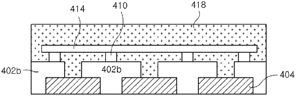
a first land comprising a first land section comprising a first height and a second land section comprising a second height that is different than the first height, wherein the first land section and the second land section meet at an internal part of the first land that defines a bottom portion of the second land section; and
a first mold encapsulant disposed adjacent a first lateral portion of the first land section and disposed below the bottom portion of the second land section, wherein a first lateral end of the second land section is devoid of the first mold encapsulant;
a semiconductor device coupled to the substrate, wherein the semiconductor device comprises:
a first side,
a second side opposing the first side, and
an outer perimeter, wherein:
the semiconductor device further comprises a first conductive bump structure disposed adjacent the first side, wherein:
the first conductive bump structure is attached to the second land section;
the first land section is disposed outside the outer perimeter of the semiconductor device; and
the first lateral end of the second land section is inside the outer perimeter of the semiconductor device; and
a mold member encapsulating at least portions of the semiconductor device, wherein:
the mold member and the first mold encapsulant comprise different materials,
the mold member directly contacts and encapsulates the first lateral end of the second land section;
the first land section comprises a first land section lower surface;
the first land section has a first width proximate to the first land section lower surface in a first cross-sectional view;
the second land section comprises a second land upper surface;
the second land section has a second width proximate to the second land upper surface in the first cross-sectional view; and
the second width is less than the first width.
|