| CPC H01L 23/49513 (2013.01) [H01L 21/4871 (2013.01); H01L 23/49503 (2013.01); H01L 23/49548 (2013.01); H01L 23/49568 (2013.01); H01L 23/49582 (2013.01); H01L 2224/32245 (2013.01)] | 20 Claims |
|
1. A method of semiconductor die attachment, comprising:
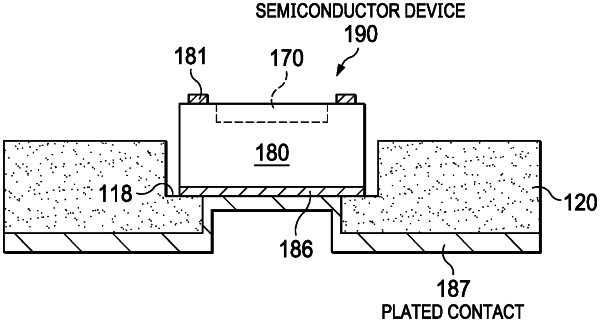
providing at least one metal substrate including a top cavity portion that is sized with area dimensions to receive a semiconductor die having a top side with bond pads thereon and a back side with a metal (BSM) layer thereon;
forming a through-hole aperture including a multi-size cavity by removing metal from an area portion of the top cavity portion and from a bottom cavity portion to form a first ring around the bottom cavity portion;
inserting the semiconductor die top side up to place the BSM layer on the first ring, and
immersing at least the BSM layer of the semiconductor die and a bottom side of the metal substrate into a plating container that provides an electroplating bath including an electroplating solution to plate a metal die attach layer that directly contacts at least a portion of the BSM layer, sidewalls of the bottom cavity portion, and a bottom side of the metal substrate.
|